![]()
When Error Is Not an Option.
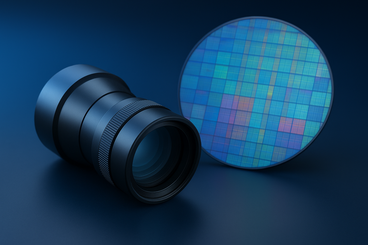
Telecentric Lenses: The Zero-Error Optical Foundation for Semiconductor & AI Vision
When measurement tolerance hits the micron level, every optical decision becomes mission critical. Telecentric optics remove the uncertainty at the source—before your algorithm ever sees the image.
Are These "Critical" Details Haunting Your Daily Operations?
Images below show common failure modes from conventional optics — distortion, hotspots, defocus and inconsistent data for AI training.

What you need isn’t just better algorithms—it's image truth from the source.
Real Parameter Comparison: Rapixel / Vision Datum vs Other Brands
Below is a concise, engineering-focused comparison pulled from lab tests and field deployments — useful when selecting optics for metrology and inspection.
| Comparison Factors | Rapixel | Other Brands |
|---|---|---|
| Optical Distortion | <0.01% — ultra-low distortion | Distortion of 0.05%–0.2% |
| Depth of Field (DOF) | Customizable DOF based on specific application needs | Moderate, prone to defocus |
| Resolution / Clarity | Supports sensors up to 151MP and 24K line sensors | Mostly up to 16MP sensor resolution |
| Max Field of View (FOV) | Up to 390mm — suitable for large PCBs, LCDs, full panel inspection | 80–160mm common |
| Sensor Support | Covering sensor sizes from 1/2.5" to full-frame (88mm image circle) | Limited, mainly for 2/3" and 1" |
| Magnification | 0.024X – 8X | Narrow options, low flexibility |
| Reliability (Annual Failure Rate) | <0.01% | 0.1% – 5% |
| Interface Compatibility | C-mount, F-mount, M42 / M58 / M72 / M90 / M95 — full coverage | Mostly C-mount |
| Wavelength Capability | Covering Visible → SWIR → UV telecentric; full-spectrum solutions for semiconductor & metrology | Limited or no SWIR/UV support |
| Proven Mission-Critical Adoption | Trusted in world-class AI and precision inspection projects; strong track record in semiconductor, IC subsurface imaging, Li-battery inspection, high-precision metrology | Mostly used in basic measurement or general-purpose inspection |
| Cost-Effectiveness | Exceptional value for precision-critical applications at competitive terms | Low cost but poor performance; priced 2–5x higher without added value |
| Support & Service | Global delivery / 3–7 working days lead time; tens of thousands of telecentric automation projects annually | Unreliable; rare reference cases |
Note: Values above reflect typical product capabilities and field performance observations. For exact model specs, check product datasheets.
Why Choose Us? — Exclusive Optics for Challenges Beyond Standard Lenses
We don’t sell "better cameras" — we deliver an optical foundation that removes measurement uncertainty. Below are three pillars of our value.
UNMATCHED: UV / SWIR / Bi-Telecentric
Full-spectrum telecentric capability enables inspection and materials differentiation that standard optics cannot achieve.
PRECISION: Ultra-Low Distortion & Native Polarization
Designs delivering <0.01% distortion and integrated polarization options for reflective-surface inspection.
PARTNERSHIP: End-to-End Integration Support
From lens selection, light-source design, camera pairing to on-site tuning and calibration—we support deployment at scale.
Ready to eliminate optical uncertainty?
Request a tailored telecentric solution for your application — sample testing and integration support available.
Share:
Empowering Plant Phenotyping with Hyperspectral Imaging — Rapixel Leads the Next Era of AgriTech Innovation
High-Resolution AOI Inspection Solutions