
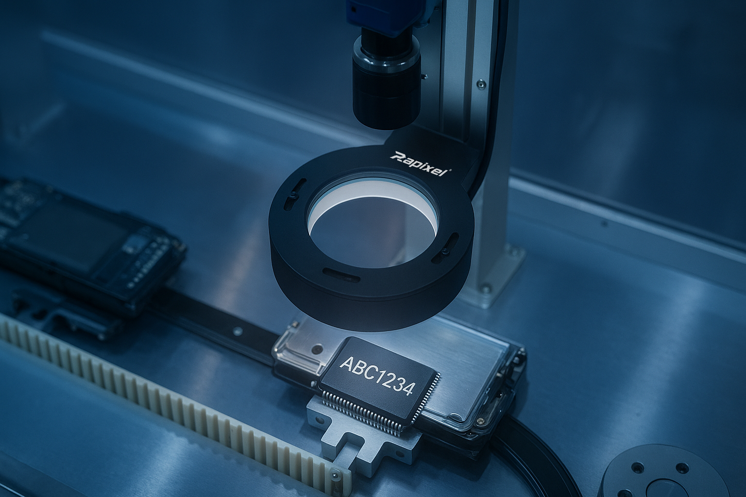
For system integrators developing Automatic Optical Inspection (AOI) solutions, chip marking inspection is a common yet demanding task. Markings on ICs are essential for traceability, quality control, and counterfeit prevention—but inconsistent quality, reflective surfaces, and high throughput requirements often complicate reliable inspection.
Common Challenges in Chip Marking AOI
-
Positioning & Alignment
Chips may be misaligned, tilted, or densely packed, requiring high resolution without sacrificing field of view. -
Surface & Marking Quality
Markings can be shallow, distorted, or inconsistent. Reflective chip surfaces introduce glare, reducing contrast. -
Recognition Accuracy
OCR engines struggle with variable fonts, damaged markings, or distorted characters. In high-speed production, integrators need low-latency imaging that maintains accuracy.
How to Overcome These Challenges
1. Choosing the Right Camera
- Area Scan Cameras are ideal for tray-based or static inspection.
- Line Scan Cameras excel in continuous conveyor-based inspection, delivering high resolution at production speed.
- High Dynamic Range (HDR) sensors ensure both bright and dark areas are captured without losing detail.
2. Optimizing Lenses for Stability
- Telecentric lenses eliminate perspective distortion, critical for measuring and recognizing small, precise markings.
- High-quality industrial lenses ensure uniform sharpness across the field of view—important when multiple chips are captured in one image.
3. Mastering Illumination
- Coaxial lighting reduces glare on reflective packages.
- Dark-field lighting highlights shallow engravings or textured markings.
- Multi-wavelength illumination combined with optical filters can significantly boost contrast on difficult surfaces.
By combining the right illumination with your chosen camera and lens, integrators can maximize contrast and recognition stability across different chip materials and marking techniques.
From Proof of Concept to Production
System integrators know that what works in the lab doesn’t always work on the production floor. That’s why it’s essential to:
- Test with real customer samples early in the design process.
- Use modular components (cameras, lenses, lighting) that can be swapped as marking or material conditions change.
- Implement synchronized triggering to ensure sharp images on high-speed lines.
- Provide maintenance-friendly setups: easy-to-clean lenses and stable, long-life illumination.
Why This Matters for System Integrators
Integrators are under pressure to deliver AOI solutions that are:
- Reliable: high inspection accuracy, even under variable conditions.
- Scalable: adaptable to different chip types, materials, and marking methods.
- Cost-effective: reducing downtime and service costs with durable, industrial-grade components.
By selecting the right camera, lens, and lighting combinations, integrators can shorten project timelines, reduce troubleshooting, and deliver inspection systems that stand out in terms of both performance and stability.
Conclusion
Chip marking inspection is one of the most detail-sensitive tasks in AOI. But with the right imaging components—optimized cameras, distortion-free lenses, and application-specific illumination—system integrators can build inspection systems that meet today’s production challenges with confidence.
Our portfolio of industrial cameras, precision lenses, and tailored lighting solutions is designed to help integrators tackle these challenges head-on. Whether you are prototyping a new AOI setup or scaling for high-volume production, we can support you with proven components and application know-how.
Share:
Revolutionizing Industrial Automation: Unlocking the Power of AI Vision Cameras
How Industrial Cameras Revolutionize Pharmaceutical Quality Control